
 6 hours ago
1
6 hours ago
1
.jpeg)
- Advertisement -

The study benchmarks emerging integration methods and materials against industry standards, offering a clear path toward ultra-low-power, high-performance transistors that could drive the next wave of AI and advanced computing.
 CMOS logic technology roadmap and potential of angstrom-scale 2D transistors. Credit: Nature Electronics, originally published in Nature Electronics
As silicon CMOS technology nears its physical limits at sub-nanometer scales, 2D semiconductors are emerging as a leading candidate for sustaining Moore’s Law. Unlike bulk silicon, these materials maintain robust electrical characteristics even at atomic thickness, making them prime contenders for future chip scaling. Major semiconductor players — including Samsung, TSMC, Intel, and IMEC — have already embedded 2D transistor development into their roadmaps for the post-silicon era, aiming for adoption by the mid-2030s.
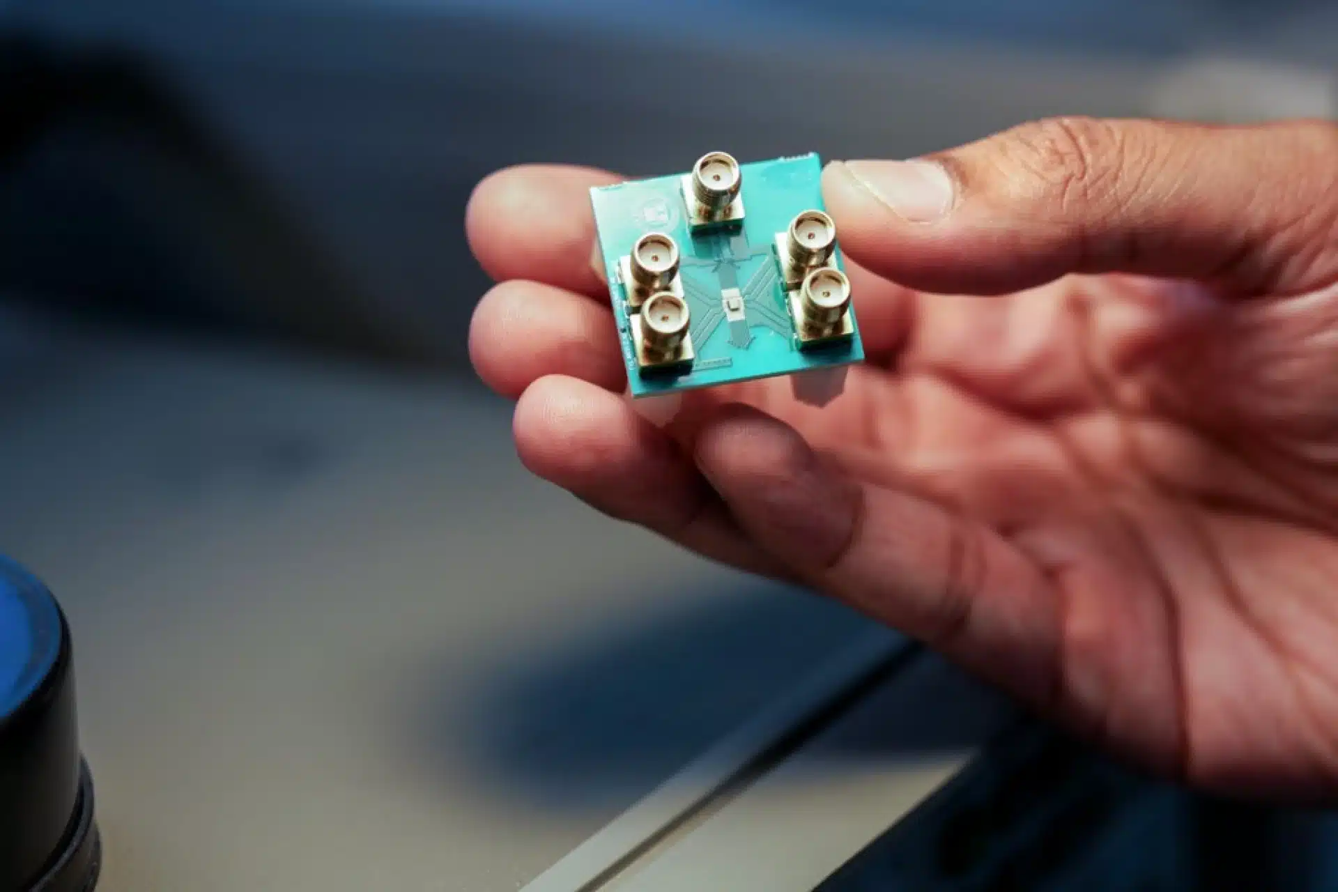
A research team from Seoul National University (SNU) has unveiled a detailed roadmap for next-generation “gate stack” technology — a key component in advancing two-dimensional (2D) semiconductors beyond the limits of silicon-based transistors. The study, led by Professor Chul-Ho Lee from SNU’s Department of Electrical and Computer Engineering, appears in Nature Electronics and offers a comprehensive blueprint for future device integration.
Yet, a critical hurdle remains: gate stack integration. The gate stack, which controls current flow in transistors, dictates device performance and reliability. Applying traditional silicon processes to 2D materials often leads to dielectric degradation, interface defects, and leakage issues — underscoring the need for entirely new material systems and process strategies tailored to atomically thin channels.
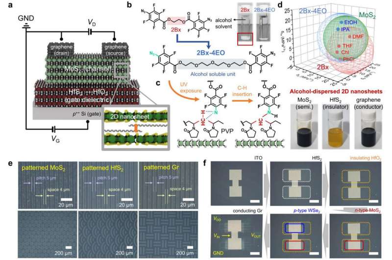
The team benchmarked existing and emerging gate stack approaches against key performance metrics, including interface trap density, equivalent oxide thickness, and gate leakage. The study classifies integration methods into five distinct categories — van der Waals (vdW) dielectrics, vdW-oxidized, quasi-vdW, vdW-seeded, and non-vdW-seeded — and maps each against the International Roadmap for Devices and Systems (IRDS) targets.
The analysis highlights promising directions such as ferroelectric gate stacks that could enable ultra-low-power logic, non-volatile memory, and in-memory computing. The roadmap also stresses real-world feasibility through Back-End-of-Line (BEOL) compatibility, low-temperature deposition below 400°C, and wafer-scale uniformity.By quantitatively comparing gate stack technologies and aligning them with industrial standards, the research offers a foundational guide for future 2D transistor design. Its insights are expected to accelerate the development of AI chips, energy-efficient mobile processors, and ultra-dense server hardware — paving the way for the semiconductor industry’s post-silicon evolution.


.jpeg)


 English (US) ·